Technology
Sony and TSMC Plan $6.4 Billion Image Sensor Plant in Kumamoto
Sony and TSMC are in talks to build a next-generation image sensor plant in Kumamoto, Japan, with an investment of about $6.4 billion.
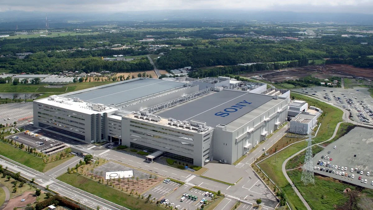
Sony Group and TSMC are reportedly planning to form a joint venture to mass produce next generation image sensor chips in Kumamoto Prefecture, Japan. According to a Nikkei Asia report cited by Techmeme, the joint venture would be owned about 60 percent by Sony and 40 percent by TSMC, with an investment of $6.3 billion. Mass production is targeted to begin as early as 2029. Bloomberg Technology reported a slightly different figure, citing a person familiar with the matter, with a combined investment of about 1 trillion yen, or $6.4 billion. The reports indicate that the two companies are in talks to realize the image sensor plant.
The discrepancy between $6.3 billion and $6.4 billion is likely due to currency fluctuations, but fundamentally both reports confirm nearly identical investment scales. This plan marks a significant step for Sony, which is known as a global leader in the CMOS image sensor market, widely used in smartphone cameras and digital cameras. By partnering with TSMC, the world's largest semiconductor foundry, Sony aims to secure advanced production capacity for next generation sensor chips. TSMC already has a production facility in Kumamoto through its subsidiary Japan Advanced Semiconductor Manufacturing (JASM), a joint venture with Sony and Denso. Kumamoto has become a hub for semiconductor investment in Japan in recent years.
The presence of TSMC in the region has attracted significant attention as the Japanese government actively promotes the rebuilding of its domestic chip industry through subsidies and incentive policies. The new image sensor plant would be an important addition to the growing semiconductor ecosystem in the Kyushu region, often dubbed "Silicon Island" due to its concentration of chip industries. Sony's majority ownership of 60 percent in the joint venture indicates its desire to maintain control over its image sensor technology, which is the backbone of its electronics components business. Meanwhile, TSMC's 40 percent stake gives Sony access to TSMC's cutting edge manufacturing process technology, including the possible use of more advanced process nodes to enhance sensor performance.
Image sensors are key components in the smartphone industry, autonomous vehicles, and IoT devices. Demand for high quality sensors continues to rise with the development of computational photography capabilities in mobile devices and the increasing adoption of advanced driver assistance systems (ADAS) in vehicles. This substantial investment reflects the two companies' confidence that demand will continue to grow in the long term. For TSMC, this partnership strengthens its position in Japan and expands its customer base beyond the logic processor segment. Although TSMC is primarily known as a manufacturer of logic chips for CPUs, GPUs, and AI applications, its manufacturing capabilities can also be leveraged to produce image sensors with more advanced processes.
This diversification could help TSMC reduce its reliance on certain segments and strengthen its overall business resilience. The Japanese government is likely to welcome this investment as it aligns with the national strategy to strengthen economic security and semiconductor supply chain resilience. Japan has allocated substantial funds to support domestic chip production, including subsidies for the TSMC plant currently under construction in Kumamoto. This new investment could potentially receive similar support, although no official announcement has been made regarding government incentives for this project. The report comes amid intensifying global competition in the semiconductor industry, particularly among the United States, China, and Taiwan.
Japan is seeking to position itself as a reliable partner in the chip supply chain, and the collaboration between Sony and TSMC is a concrete example of these efforts. By producing image sensors in Japan, the two companies can reduce the risk of supply chain disruptions that may arise from geopolitical tensions in the Taiwan Strait. Neither Sony nor TSMC has officially confirmed the details of this joint venture. The two companies are still in the discussion stage, according to Bloomberg's source. If realized, this project would become one of the largest foreign investments in Japan's semiconductor sector and mark a new chapter in Japan Taiwan industrial relations.
The project also reflects a broader trend where major technology companies are increasingly choosing to secure chip production capacity through strategic partnerships with leading foundries. This model allows companies like Sony to focus on design and product innovation while leveraging the manufacturing expertise of partners like TSMC. The success of this model in Kumamoto could serve as a blueprint for similar collaborations in the future. With production targeted as early as 2029, there is still about three years to complete negotiations, facility construction, and equipment installation. Such projects typically take years from planning to mass production, especially for next generation image sensor technology that requires high precision manufacturing processes.
Further developments of this plan will be an important indicator for the direction of the global semiconductor industry and Japan's position within it.